Device technology and scalability
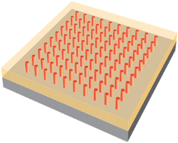
Topical area C will focus on the potential for miniaturization of resistively switching devices, which requires precise control and tailoring of relevant defects or material phases at the nanometer scale. We will analyze scaling phenomena that will affect the device parameters and that eventually will encounter inherent physical limits. We will explore new concepts for highly scaled resistively switching cells as well as the engineering of active defects on the atomic scale.
From a technological perspective, the potential scalability down to the true nanometer regime holds promise for lower production cost and lower energy consumption, which are major driving forces to push the device technology to new frontiers. However, the device properties in the few-nm regime significantly differ from their μm counterpart.
For the ReRAM technology, forming voltage not only scales with insulator film thickness but also with lateral device dimensions. Variability and reliability are significantly affected by the device scaling and extrinsic influences, such as the surrounding environment (which can, for example, act as a source or sink of oxygen) will play a dominating role. These aspects will be addressed by the SFB. Another route towards higher cell densities, namely the introduction of full 3D architectures, is considered a purely technological work which will be pursued by the industry – it is no central aim of our SFB.
For the PCM technology, two aspects of scalability need to be considered: the phase change materials and the PCM devices. These aspects will strategically be analyzed in the project area C and in project Z4. On the materials side, effects of one-dimensional up to three-dimensional confinement will be studied, which includes fundamental questions on the binding properties as well as on the crystallization kinetics in confined dimensions. Furthermore, unintended phenomena, such as drifting of resistance states due to relaxation of the amorphous phase, which complicate predicting the device properties, will be taken into account.

